
Photonics Spectra discusses impact of micro LEDs on display industry

Photo of 200 mm GaN-on-Si micro LED wafer of ALLOS and overview over its superior properties

In his analysis for Photonics Spectra, Hank Hogan looks at the challenges of micro LED manufacturing and solutions to overcome the challenges – including ALLOS’ proprietary and patented process for growing gallium nitride (GaN) on large diameter silicon (Si) substrates to address the cost – and with ALLOS’ technology – also the yield challenges.
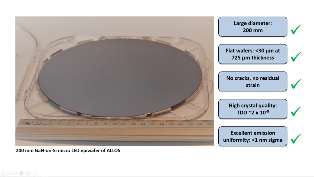
Photo of 200 mm GaN-on-Si micro LED wafer of ALLOS and overview over its superior properties

The full article is available on Photonics Spectra’s websites.
More News

ALLOS Semiconductors and Ennostar announce strategic partnership

ALLOS and Ennostar Forge Strategic Partnership to Launch 200 mm Supply Chain for MicroLEDs

Dresden, Germany / Hsinchu, Taiwan – ALLOS Semiconductors of Germany and Ennostar Corporation of Taiwan today announced a strategic partnership to bring 200 mm GaN-on-Si (gallium nitride on silicon) LED epiwafers for microLED applications into volume production. This collaboration represents a key milestone in establishing a silicon fab-compatible supply chain for microLED products.

Continue Reading